




Vicor提起第三波電源模組專利侵權訴訟,被告包含台達、廣達與鴻海
iKnow科技產業資訊室/2026-09-14/君沉吟

圖、Vicor提起第三波電源模組專利侵權訴訟,被告包含台達、廣達與鴻海
如本網站先前報導:列名台達、廣達與緯穎,Vicor再提伺服器電源模組專利侵權訴訟,台達提起反訴, 指控Vicor侵害專利與營業秘密,針對鴻海、緯創與廣達集團銷售到美國境內的人工智慧伺服器系統中所內含的電源模組產品,Vicor分別於2023年與2026年初,在美國國際貿易委員會 (USITC) 和聯邦地方法院提起兩波專利侵權訴訟。於2023年訴訟中,被告的電源模組供應商僅台達電子一家;於2026年初訴訟中,被告的電源模組供應商增加為台達電子、芯源系統 (MPS)、上海沛源電子三家。
2026年初訴訟經過半年法院攻防,原、被告雙方似乎並沒有朝和解方向發展;相反地,芯源系統和台達電子分別於2026年7月提起反訴,兩家公司都控告Vicor侵害營業秘密與各自擁有的專利權。如此可能迫使Vicor傾向主張更多專利,以對被告們施加更大壓力。
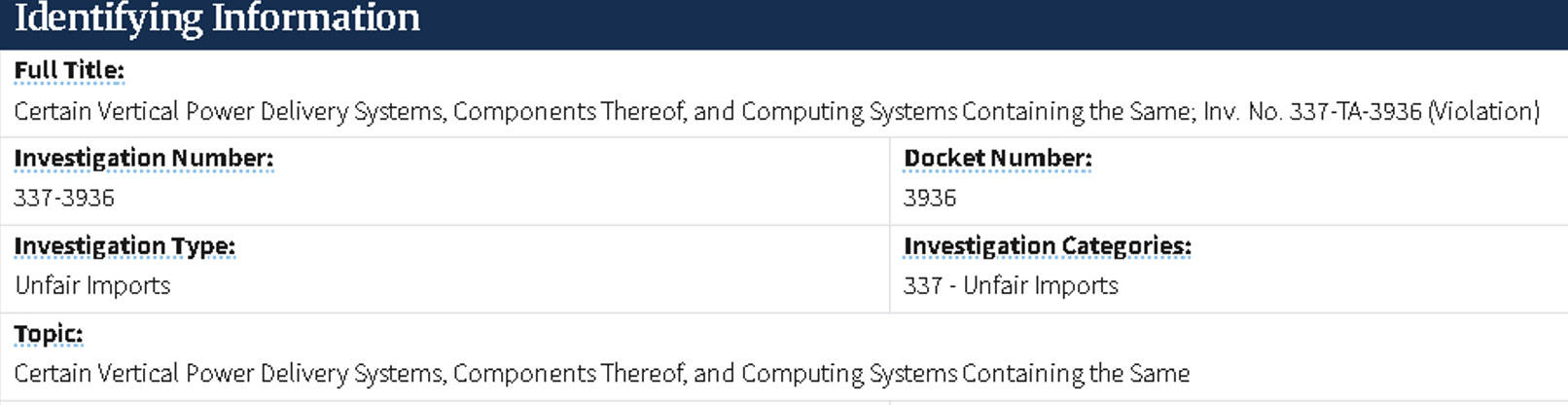
如表一、表二整理,Vicor於9月初發動第三波侵權訴訟攻擊,於美國國際貿易委員會提起編號337-3976訴訟,而於東、西德州地方法院針對不同電源模組供應商及其下游客戶分別提起三件訴訟。這波訴訟目前只主張一件與垂直電力傳輸系統 (Vertical Power Delivery Systems, 簡稱VPD) 相關的 US10903734B專利。
表一、Vicor於USITC控告台達電子、英飛凌、芯源系統侵害垂直電力傳輸系統專利訴訟
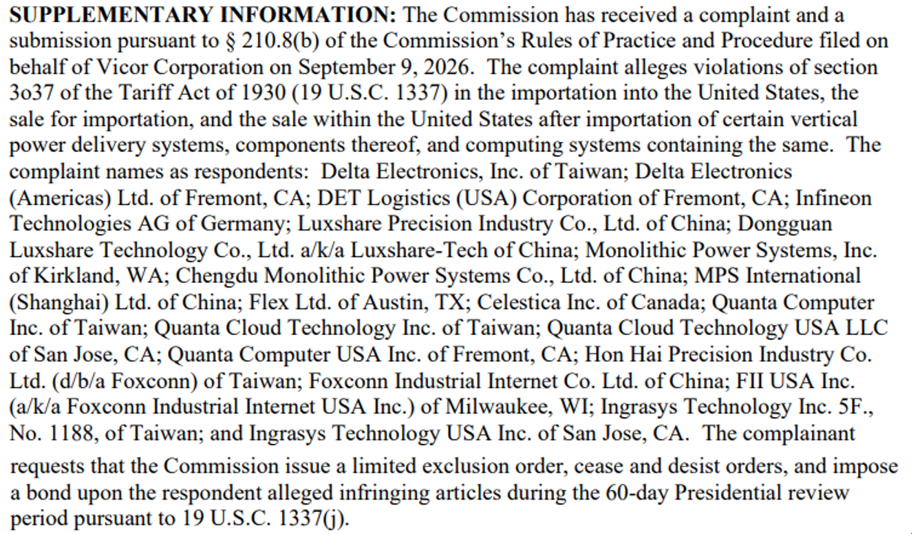
表二、Vicor於東、西德州地方法院分別控告台達電子、英飛凌、芯源系統侵害垂直電源模組專利訴訟
| Case | Filing Date | Court | Plaintiff | Defendant |
| 2:26-cv-00796 | 2026/9/7 | Texas Eastern District Court |
Vicor Corp | Infineon Technologies AG Hon Hai Precision Industry Co Ltd Quanta Computer Inc Delta Electronics (americas) Ltd Foxconn Industrial Internet Co Ltd Luxshare Precision Industry Co Ltd Dongguan Luxshare Technology Co Ltd A/k/a Luxshare-Tech Delta Electronics Inc Quanta Cloud Technology Inc Ingrasys Technology Inc Celestica International Inc |
| 7:26-cv-00364 | 2026/9/7 | Texas Western District Court | Vicor Corp | Monolithic Power Systems Inc Chengdu Monolithic Power Systems Co Ltd MPS Holding BV |
| 7:26-cv-00365 | 2026/9/7 | Texas Western District Court | Vicor Corp | Flex Ltd |
US10903734B 專利範圍
針對第三波被告的產品,Vicor於訴訟中多主張侵害US ‘734B專利的第一項申請專利範圍;如表三、圖一整理,筆者列出該專利第一項申請專利範圍原文及其翻譯,並把第一項申請專利範圍相關元件自專利說明書對應圖式中註記標示出來,以方便讀者理解。
表三、US10903734B 專利第一項申請專利範圍及其翻譯
| US10903734 | claim 1 中文翻譯 | |
| 1.pre | 1. A method of powering a semiconductor device having power input terminals, the method comprising: | 1. 一為具有電源輸入端子的半導體裝置供電的方法,該方法包括: |
| 1.a | providing a power conversion module having conversion circuitry arranged in a multi-cell structure having a plurality of conversion cells, | 提供一電源轉換模組 310,該電源轉換模組具有以多單元結構佈置的轉換電路 converter 20,該多單元結構具有多個轉換單元 250-1~250-n, |
| 1.b | each conversion cell including one or more converter output terminals, | 每個轉換單元包括一個或多個轉換器輸出端子 Fig. 2 電路: 227-1~227-n;Fig. 5 機構: 312、313; |
| 1.c | the conversion circuitry being configured to convert power received at a first voltage for delivery via the converter output terminals of the plurality of conversion cells at a second lower voltage, | 該轉換電路 20 配置為: 將以第一電壓 Vin 接收的電能,轉換為在多個轉換單元的轉換器輸出端子,以第二較低電壓 Vout 輸出的電能, |
| 1.d | the converter output terminals being arranged in a first pattern having a first spacing between the converter output terminals; | 該轉換器輸出端子 312、313 以第一排列方式設置,於該第一個排列方式下,該轉換器輸出端子之間具有第一間距; |
| 1.e | providing an interconnection module having x-input terminals arranged on a first side of the interconnection module in a pattern configured to align with the first pattern of converter output terminals, and | 提供一互連模組 350,該互連模組的第一側設置有 X 輸入端子 362、363,其排列方式與轉換器輸出端子 312、313 的第一排列方式一致; |
| 1.f | x-output terminals arranged on a surface of a second opposite side of the interconnection module in a second pattern configured to align with the power input terminals of the semiconductor device, the second pattern having a second spacing between x-output terminals, | 該互連模組的第二相對側的表面上設置有複數個 X 輸出端子 364,該複數個 X 輸出端子以第二排列方式設置,如此第二排列與半導體器件的電能輸入端子一致,於該第二排列方式下,該X輸出端子364之間具有第二間距, |
| 1.g | the second spacing being different than the first spacing, the x-input terminals being electrically connected to the x-output terminals; | 該第二間距與第一間距不同,並且X輸入端子與X輸出端子電連接; |
| 1.h | assembling the power conversion module to the first side of the interconnection module with each converter output terminal mated with and electrically connected to a respective x-input terminal; | 將電源轉換模組310組裝到互連模組350的第一側,使每個轉換器輸出端312、313與對應的 X輸入端子362、363對齊並電連接; |
| 1.i | wherein the interconnection module is configured to provide electrical and mechanical translation between the converter output terminals arranged in the first pattern and the power input terminals of the semiconductor device arranged in the second pattern; | 其中,互連模組配置350用於 “在第一排列方式設置的轉換器輸出端子312、313” 與 “第二排列方式設置的半導體元件的電能輸入端子” 之間提供電氣和機械轉換; |
| 1.j | wherein the power conversion module and the interconnection module are stacked to form a module sandwich including the power conversion module in a first layer, electrical connections between the converter output terminals and the x-input terminals in a second layer, and the interconnection module in a third layer. | 其中,功率轉換模組310和互連模組350堆疊形成模組三明治,包括第一層中的功率轉換模組310 、第二層中的轉換器輸出端子312、313 與X輸入端子362、363之間的電連接、以及第三層中的互連模組350。 |
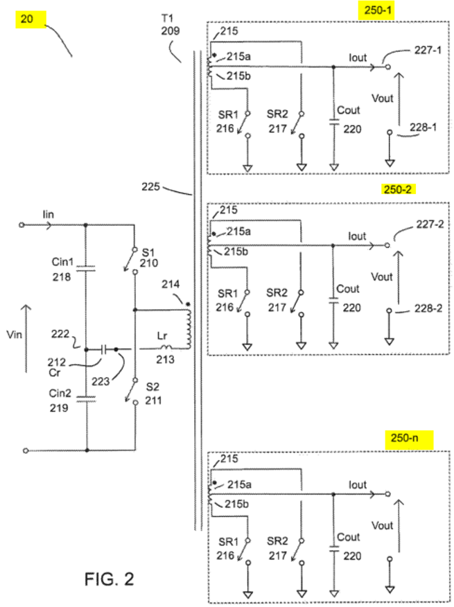
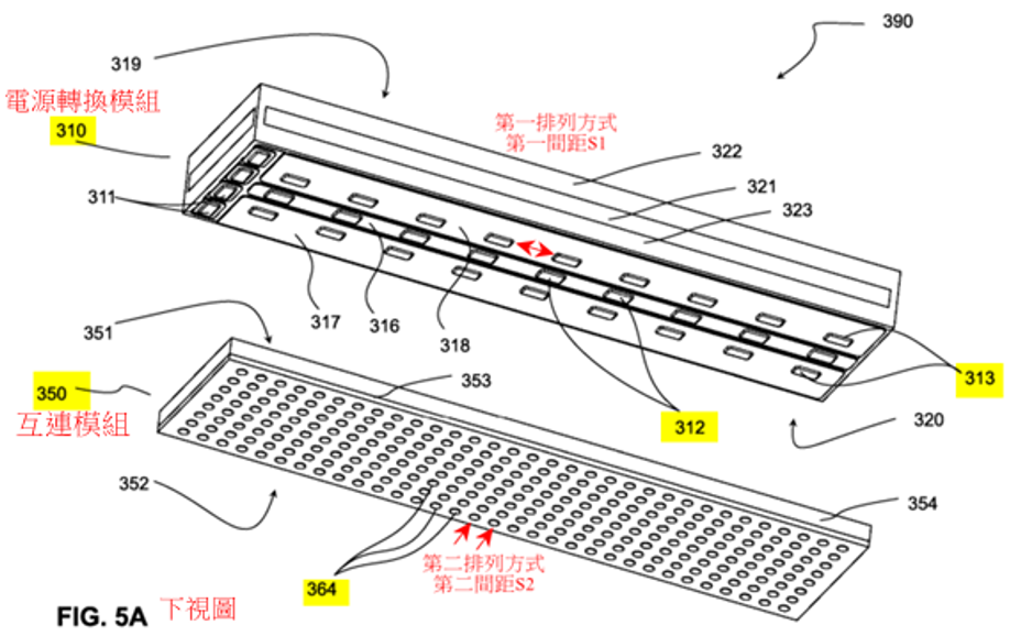
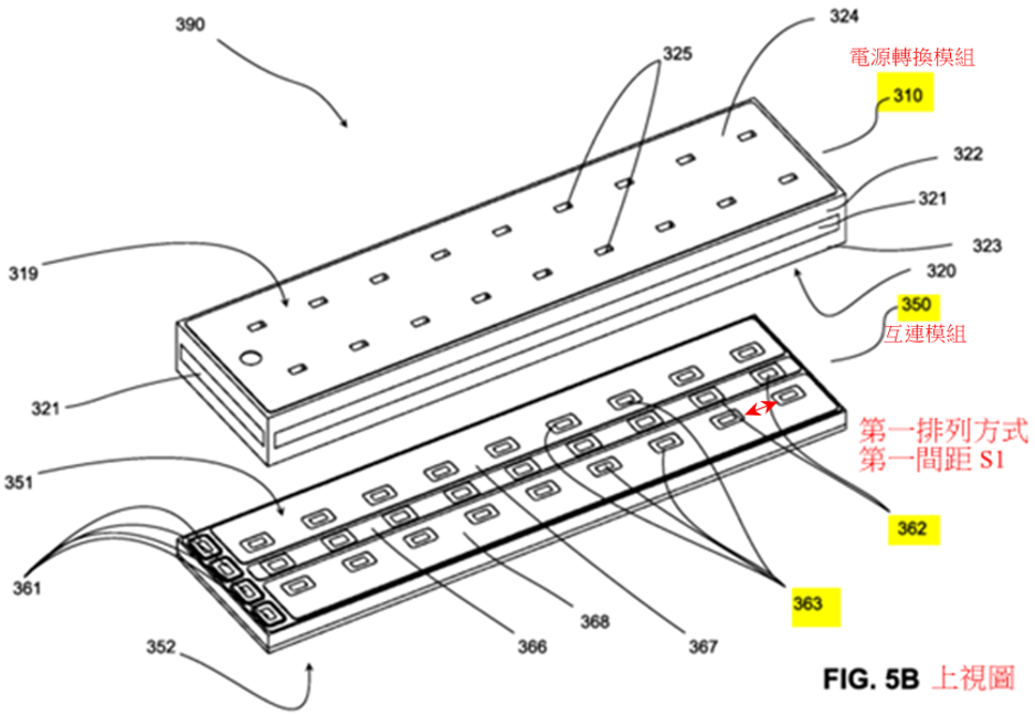
圖一、US10903734B 專利第一項申請專利範圍元件相關圖式註記
US10903734B 專利第一項申請專利範圍與英飛凌產品侵權比對
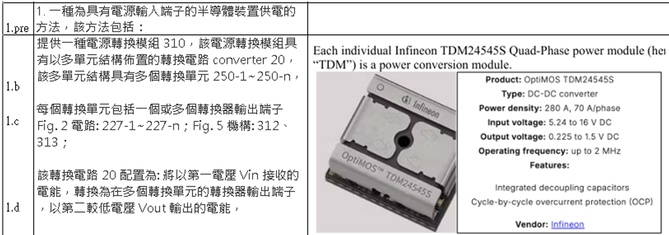
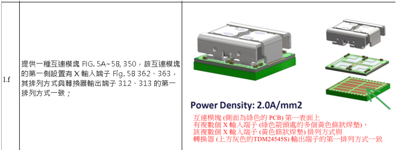
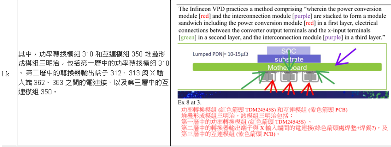
如表四整理,筆者於左欄列出該專利第一項申請專利範圍翻譯,並於右欄列出Vicor於地院訴狀附件七所提供與英飛凌產品侵權比對表 (claim chart) 部分截圖,並加註部分中文說明以方便讀者理解。如圖二,筆者補充Vicor舉證英飛凌電源模組產品參展影片的額外截圖,方便讀者理解英飛凌電源模組產品中,印刷電路板垂直投影相對兩面,分別設置 “多個轉換單元” 與 “GPU焊墊”。
表四、US10903734B 專利第一項範圍圍與英飛凌產品侵權比對
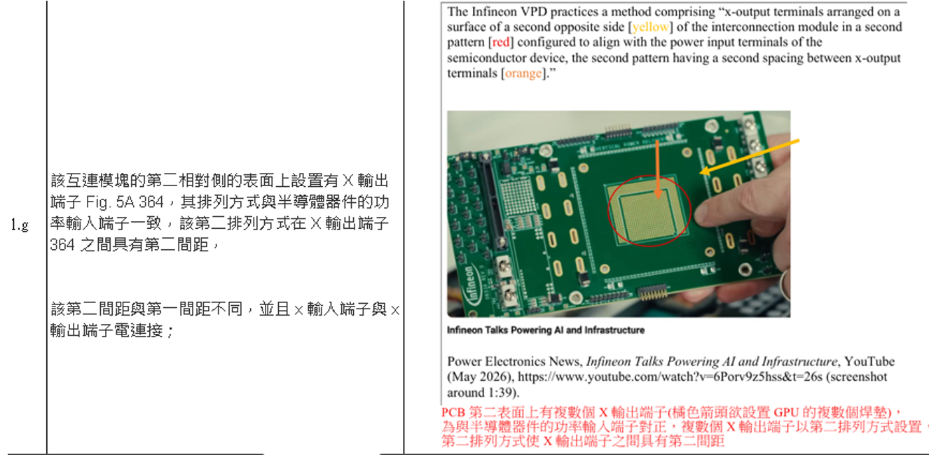
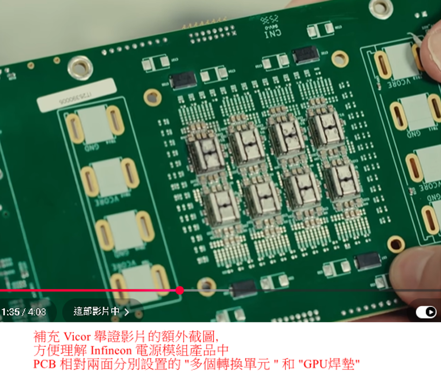
圖二、英飛凌電源模組產品參展影片的額外截圖
結語
針對Vicor今年初訴訟訴狀附件的侵害分析比對表,台達電子和芯源系統於今年7月中,都提起侵害營業秘密反訴,主張Vicor是以不正當手段取得台達電子和芯源系統的機密技術文件,如此據以進行專利侵害比對。
因此,Vicor於提起此次的第三波訴訟時,想必是格外小心,確定只依據公開資料來準備呈堂證據;也因此才會連英飛凌參展的事業處主管訪談YouTube影片都被截圖作為侵權比對的部分證據。(2226字;圖1)